Research Background
When materials are made into nanoparticles, they sometimes exhibit properties that are different from those of their bulk counterpart. One example is a decline in the melting point, which means that even metals could have lower melting points as they become extremely small nanoparticles. In other words, the melting point is not “unique to each material” but depends on both the type of material and the size. This theme is important in nanoscience and nanoengineering. When metal conductivity is sought by annealing, it is possible to lower the annealing temperature even at a little larger scale than the nano one. It is possible to create an electroconductive material that contributes to the printed electronics field by taking advantage of this feature.
Our lab has already widely conducted research on metal nanoparticles and fine particles and has explored their application potentials to electronics with the aim of developing commercial applications.
Research Theme
– Synthesize non-oxidized transition metal fine particles and nanoparticles and use them as raw materials for electronics.
After preparing transition metal particles such as copper and nickel by a chemical reduction process, we obtain metal nanoparticles with a consistent particle size and anti-oxidation property. Our lab has already succeeded in fabricating copper materials of consistent size from the cluster level to particle level with sizes of approximately 200 nm. As described in other web pages, we use various methods to synthesize nanoparticles, including the chemical reduction process, plasma in liquid process, and matrix sputtering process.
Published Papers
- 成島隆, 吉岡隆幸, 宮崎英機, 菅育正, 佐藤進, 米澤徹 、「マイクロ波液中プラズマ法による銅 微粒子の合成」、日本金属学会誌、76(4), 229-233 (2012). 2)
- Kiyonobu Ida, Masanori Tomonari, Yasuyuki Sugiyama , Yuki Chujyo , Tomoharu Tokunaga, Tetsu Yonezawa, Kotaro Kuroda, Katsuhiro Sasaki, “Behavior of Cu nanoparticles ink under reductive calcination for fabrication of Cu conductive film”, Thin Solid Films, 520, 2789–2793 (2012)
- Tetsu Yonezawa, Naoki Nishida, Atsushi Hyono, “One-pot Preparation of Antioxidized Copper Fine Particles with a Unique Strucure by Chemical Reduction at Room Temperature”, Chem. Lett. , 39, 548-549 (2010).
- 西田直樹、米澤 徹、 「第1章 金属ナノ粒子の種類、合成法分類と基本的な物性」(分担執筆) 菅沼克昭監修「プリンテッドエレクトロニクス技術最前線」、シーエムシー出版、pp. 115-120 (2010).
- 兵野篤・米澤徹、 「金属ナノ粒子・微粒子の湿式合成法と応用」、 セラミックス、45(8), 609-612 (2010)
- Masanori Tomonari, Kiyonobu Ida, Hiromi Yamashita, Tetsu Yonezawa, “Size-controlled oxidation-resistant copper fine particles covered by biopolymer nanoskin”, Journal of Nanoscience and Nanotechnology, 8(5), 6925-6927 (2008).
Application example
Among these, copper fine particles synthesized by the liquid reduction process have found wide-ranging commercial applications in inks and pastes. There are not many systems that can create copper nanoparticles of such a small size in powder form and in a non-oxidized state, and we believe our system is superior to those found elsewhere. We use gelatin as a dispersant. Gelatin densely coats the surfaces of the copper fine particles and prevents their oxidization.
Gelatin exhibits a small “gold number” (the index indicating the amount of a dispersant required for continuing dispersion of gold nanoparticles even after NaCl is added), excellent protective capacity, and low oxygen permeability and is inexpensive. Therefore, it is considered to be suitable for such purposes.
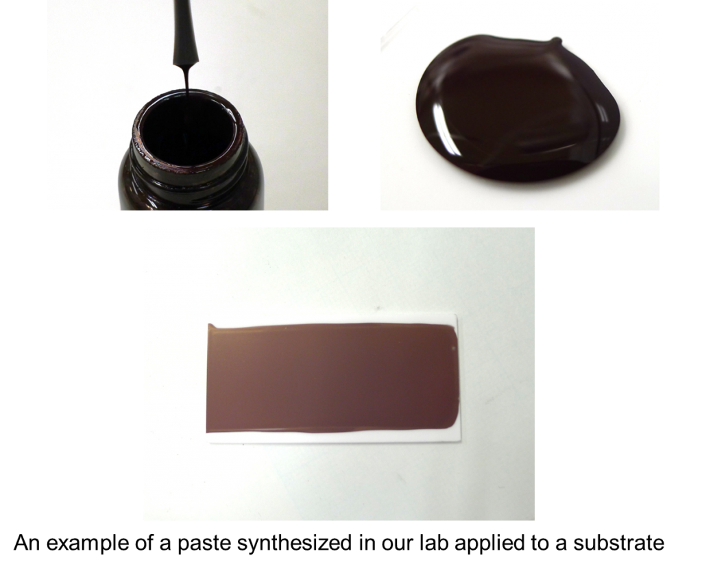
In addition to particle synthesis, recently, we have been making increased efforts to create more uniform ink and paste. Furthermore, we are observing interesting variations in, for example, the melting process and annealing behavior, which has great potentials for enabling the supply of copper nanomaterials that satisfy demand from the industry. In many cases, pasting fine particles or nanoparticles requires certain know-how; we are also developing such know-how. In fact, we own a device for making paste, as shown on the “Facilities” page.
We believe that not many universities put such vigorous efforts into commercial applications. We are confident that our research is cutting-edge even in the world in terms of the practicability of copper nanomaterials. We plan to aggressively file patent applications and present and publish our papers while exploring new atom-substitution and cost-reduction (e.g., nickel to copper and silver to copper) opportunities for electroconductive materials.
It is our ambition to play a significant role in the development and expansion of the field of printed electronics, which is expected to experience a huge leap in the future.
These copper fine particles are used not only for conductive thin layers and wiring printing but also for the inner electrodes of multilayered ceramic capacitors (MLCC). Nickel has been increasingly employed in the inner electrodes in MLCCs, replacing Ag-Pd alloys. Nickel, however, suffers from several shortcomings, and substitution by copper has been considered. We believe that the substitution of the rare metal nickel with the common metal copper to avoid nickel’s magnetism and toxicity is one of the most important challenges in the electronic parts industry, though price motivation is low.
The formation of copper wiring can be easily achieved by laser direct writing using copper fine particles. Furthermore, we will be able to produce copper fine particle paste that can be used in conjunction with all types of sintering from low-temperature sintering and manufacturing of glass ceramics at a temperature of approximately 600 ˚C to high-temperature sintering for MLCC inner electrodes and laser sintering.
Published Papers
- Gang Qin, Akira Watanabe, Hiroki Tsukamoto, and Tetsu Yonezawa
“Copper Film Prepared from Copper Fine Particle Paste by Laser Sintering at Room Temperature: Influences of Sintering Atmosphere on the Morphology and Resistivity”
Japanese Journal of Applied Physics, in press. - Tetsu Yonezawa, Shinsuke Takeoka, Hiroshi Kishi, Kiyonobu Ida, Masanori Tomonari, “The preparation of copper fine particle paste and its application as the inner electrode material of a multilayered ceramic capacitor”, Nanotechnology, 19(14), 145706 (2008).
We are making in-situ observations of fine particles and nanoparticles at high temperatures. For more information, please see the section “In-situ heating TEM”

